Overview
The LC9997M is a 1/5-inch optical size frame transfer
CCD solid-state image sensor.
Features
∑ Effective pixels [total pixels]: 508
◊
246 [532
◊
250] (H
◊
V)
∑ Number of optical black pixels:
Horizontal: 2 in front, 22 in back
Vertical:
2.5 above, 1.5 below
∑ Dummy bits: Horizontal: 4 pixels
∑ Horizontal resolution: 330 TV lines
∑ Small form factor supports compact application products
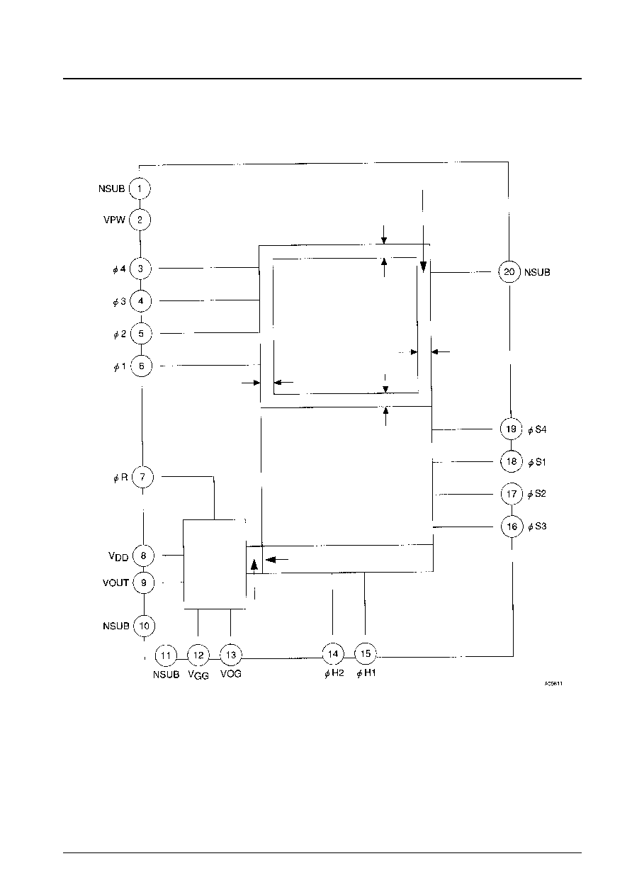
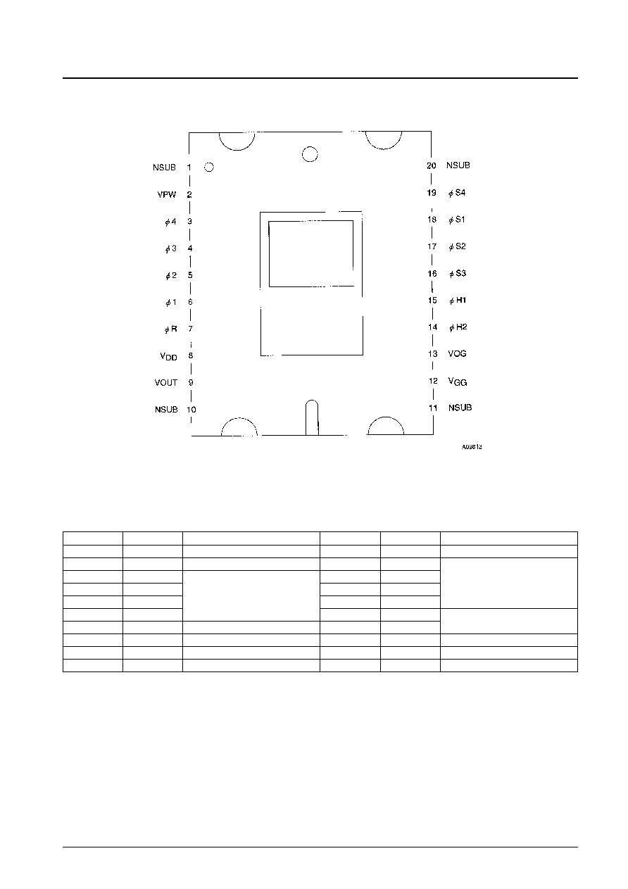
∑ 20-pin half-pitch transparent DIP package
∑ Horizontal shift register operates at 5 V.
∑ Supports variable-speed electronic shutter operation.
Device Structure
∑ 1/5-inch optical size frame transfer CCD image sensor
∑ Unit cell size: 5.8 µm
◊
9.0 µm (H
◊
V)
∑ Chip size: 4.18 mm
◊
5.10 mm (H
◊
V)
∑ Parallel gate CCD sensor
∑ Built-in high-sensitivity output amplifier
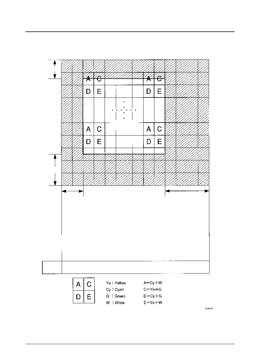
∑ Cy-G-Ye-W mosaic complementary color filters
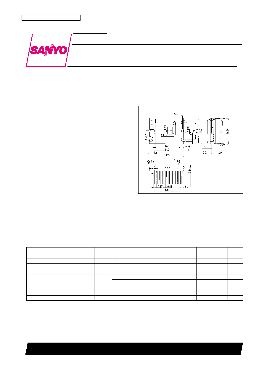
Package Dimensions
unit: mm
3217
53098RM (OT) No. 5783-1/11
Preliminary
[LC9997M]
SANYO Electric Co.,Ltd. Semiconductor Bussiness Headquarters
TOKYO OFFICE Tokyo Bldg., 1-10, 1 Chome, Ueno, Taito-ku, TOKYO, 110-8534 JAPAN
1/5-Inch Frame Transfer CCD
NTSC Color Image Sensor
LC9997M
Ordering number : EN
*
5783
Parameter
Symbol
Conditions
Ratings
Unit
Supply voltage
V
DD
V
PW
= 0 V
≠0.3 to +18
V
Load gate voltage
V
GG
V
PW
= 0 V
≠0.3 to +5
V
N substrate - p-well voltage
NSUB≠VPW
≠0.3 to +50
V
N substrate - image and storage area voltage
NSUB≠
1 to
4,
S1 to
S4
≠0.3 to +55
V
Horizontal clock pin,
R: V
PW
= 0 V
≠0.3 to +18
V
Pin voltage
Other clock pins: V
PW
= 0 V
≠15 to +18
V
Other pins: V
PW
= 0 V
≠0.3 to +10
V
Operating temperature
Topr
≠10 to +60
∞C
Storage temperature
Tstg
≠30 to +80
∞C
Specifications
Absolute Maximum Ratings
at Ta = 25∞C
No. 5783-5/11
LC9997M
Parameter
Symbol
Conditions
Ratings
Unit
min
typ
max
Imaging area pulse signals: ¯1, ¯2, ¯3, ¯4
Pulse amplitude
V
PIF
*
1
14.0
14.5
15.0
V
Low level
V
LIF
*
1
≠10.0
≠9.5
≠9.0
V
Storage area pulse signals: ¯S1, ¯S2
Pulse amplitude
V
PSL
14.0
14.5
15.0
V
Low level
V
LSL
≠8.0
≠7.5
≠7.0
V
Storage area pulse signals: ¯S3, ¯S4
Pulse amplitude
V
PSL
14.0
14.5
15.0
V
Low level
V
LSL
≠9.0
≠8.5
≠8.0
V
Horizontal transfer pulse signals: ¯H1, ¯H2
Pulse amplitude
V
PH
4.5
5.0
5.5
V
Low level
V
LH
0
0
0.5
V
Reset gate: ¯R
Pulse amplitude
V
PR
4.5
5.0
5.5
V
Low level
V
LR
4.2
4.5
4.8
V
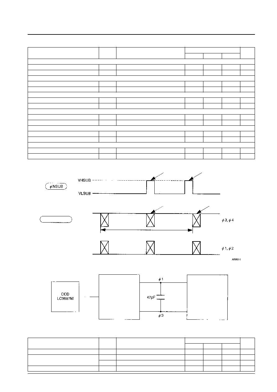
Substrate pulse: ¯NSUB
Pulse amplitude
V
HSUB
*
2. See Figure 1.
30.0
40.0
V
Low level
V
LSUB
See Figure 1.
17.5
18.0
18.5
V
Clock Voltage Conditions
at a frame shift frequency of 3.58 MHz
Notes: 1. Insert 47-pF capacitance as shown in Figure 2.
2. V
HSUB
must be adjusted so that the saturated output is maximum within the range where image degradation does not occur.
Figure 1
Figure 2
Parameter
Symbol
Conditions
Ratings
Unit
min
typ
max
P - well
V
PW
0
V
Output circuit voltage
V
DD
*
3
14.5
15.0
15.5
V
V
GG
*
4
1.2
1.5
1.8
V
OG bias
V
OG
*
4
4.5
5.0
5.5
V
Bias Conditions
Shutter pulse
Slice pulse
Charge sweep-out pulse
One field
Frame shift
Imaging area pulses
Vertical driver IC
LC89901V
Core IC
LC99053